| cosam.org |
Front Panel
Although the system itself had been operational for some time, I realised it was lacking in one specific department: no self-respecting homebrew system would be complete without a full-on blinkenlights front panel from which to probe the system at the lowest possible level. Little did I know that this seemingly simple addition would turn out to be the most challenging and complicated part of the project to date!
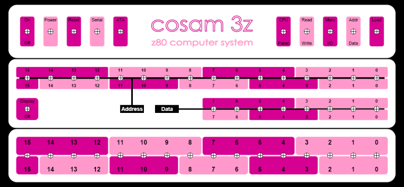
After jotting down a brief description of the requiements, I sketched a few ideas for the layout of the switches and all-important LEDs. I finally settled on the design pictured here - click for a more legible version. Fellow retro fans may recognise a passing resemblence to DEC's early PDP-11 systems which is, of course, purely coincidental. The panel does however have its bits marked up in groups of four, as hexadecimal is generally the norm in Z80 circles, as opposed to the PDP's octal representation.
Operation
The top left of the panel is bascially what I already had on the makeshift control panel, plus an extra LED which indicates activity on the serial port. The upper right section is where things start to get more interesting. From these few switches it's possible to take control of the system bus (using the Z80's /BUSREQ and /BUSACK signals) and set values on the conrtol lines, enabling the user to read from or write to memory locations or I/O ports.
In the middle of the panel are two rows of LEDs which show the current values on the address and data busses. The LEDs can be turned off using the switch to the left.
The bottom row of switches is used to input binary values into the system. An initial address can be loaded by flipping the Addr/Data switch to Addr, toggling in the value, and pressing load. The same switches (more specifically: the eight switches to the right) can then be used to input individual bytes of data by simply flipping the Addr/Data switch to Data. In order to simplify reading and writing data sequentially to or from memory, the address is automatically incremented when the load button is pressed.
Construction
Basic Hardware
The backboard of the panel was cut from a 4mm piece of MDF. I used a draft print-out of the panel taped onto this to mark the centres of all the holes with a punch before drilling these out. I then printed off a good copy of the panel graphics, laminated it, and cut out the necessary holes with a scalpel. The switches are all of the panel-mount type and therfore came with fasteners with which to attach them to the board. The data and address bus LEDs were however mounted using small bits of stripboard, along with their resistors. The black bezels visible on the photo are LED holders, but most of these are just pushed into place; The LEDs are not clipped into the back. My excuse for the less-than-straight lines is that the holes where made with a hand-held drill and were therefore subject to occasional wandering!
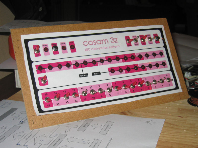 Front of the panel, with switches and LEDs mounted. |  The rear side, showing wiring and interface circuitry. |
Electronics
Designing the circuitry required to interface the front panel to the system turned out to be more challenging that initially expected. The first design involved using a few tristate latches to store the values of what would essentially be the address and data registers, plus a bit of glue logic to generate the appropriate control bus signals depending on the positions of the switches. Such a configuration would however have required much more work from the user to get anything done as the address bus would need to be toggled in for every single location. This would make sequential reading and writing very laborious.
The vital improvement was the automatic incrementation of the address on every read or write operation, as decribed above. This means a starting address can be toggled in and all subsequent reads and writes cause the address bus to skip to the next location automatically, ready for the next byte. This improvement did however add to the complexity as four 4-bit counters would be required to keep track of the value, as opposed to two 8-bit latches. Even worse, the counters can't be connected directly to the address bus, so a tristate buffer was required.
Timing
Another problem I originally underestimated was the generation of the various control signals. The real challenge has to do with something you can easily take for granted: timing. When the system is running, this is of course all handled by the CPU. However, when the panel is enabled, it essentially replaces the CPU and must therefore manage the timing itself. This means that you can't simply say that, for example, /RD is the inverse of /WR as the propagation delay of an inverter will cause both signals to become active when switching between the two, albeit for a very short period of time. These "mixed signals" can cause havoc on the system busses as devices suddenly aren't sure if they should be reading data or writing it. The result would be at best a glich or corruption of data or, at worst, broken hardware as outputs of different devices get connected to each other. Timing of the clock pulse to the address bus counters must also be accurate to prevent the address from suddenly changing in the middle of a read or write cycle.
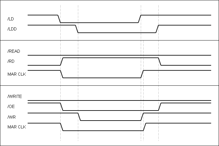 In the end, the only sane way to manage all of this was to draw up a
timing diagram of how things ought to be, then derive the logic from this.
The final version of the diagram is shown to the right - click it for a
more legible version. The uppermost part of the diagram shows the load
signal (/LD) along with a delayed "copy" of this signal called /LDD.
/LDD plays a crucial role in the timing as /LD and /LDD combined provide,
with their overlap, the "windows" in which other signals should be active.
In the end, the only sane way to manage all of this was to draw up a
timing diagram of how things ought to be, then derive the logic from this.
The final version of the diagram is shown to the right - click it for a
more legible version. The uppermost part of the diagram shows the load
signal (/LD) along with a delayed "copy" of this signal called /LDD.
/LDD plays a crucial role in the timing as /LD and /LDD combined provide,
with their overlap, the "windows" in which other signals should be active.
The middle section illustrates what should happen during a read cycle. When the Read/Write swicth is in the Read position, the /READ input is pulled low. Under normal circumstances (i.e. when the Load button is not being pressed) the /RD signal on the Z80 bus is also low, causing the data to be read from the current address and displayed on the data bus LEDs. When the Load button is pressed, the /LD line goes low and we want two things to happen: First, we want /RD to go high and, while it's still high, we want the address to be incremented. When the address has been incremented, /RD is pulled low again and the data is read again from the next address. The important point here is that the address is incremented before /RD goes low again, otherwise we'll just be reading from the non-icremented address.
Lower down we see the desired write cycle timing. This is more complex as we're dealing with two signals. It's also the opposite way around to the read cycle in that /WR is normally high and gets pulsed low during the load. To write data, the buffer between the panel switches and the data bus must to be enabled (the /OE signal). This must stay open to provide valid data while the /WR signal is pulsed low to initiate a write to the selected address. The /WR signal also has an effect on the MAR CLK signal in that /WR must be high before the rising egde of MAR CLK triggers the address counter to increment. (During a read cycle, /WR is of course always high so we can derive the MAR CLK from /LD alone.)
With the desired timing determined, the logic can be derived by matching the required signal timing to the combined states of the input signals. For example, /OE must be pulled low when both /LD and /LDD are low, but only when /WRITE is low. This is relatively complicated so in order to keep the number of parts down I used a 3-8 decoder to produce the bluk of the signals. Even with just these few signals, this can be quite a mind-bender if your boolean logic is as rusty as mine!
Timing of the /MEMRQ and /IORQ signals was solved mush more simply by using both outputs from the Memory/IO toggle switch, each producing one of the two signals. All that was required was to ensure that both signals would be high for the brief period of time that the switch moved from one position to the other.
Finishing Up
With the electronics sorted, there was also a fair amount of wiring to get done, purely due to the sheer number of components involved. I also took the trouble of debouncing the all control switches. Although this probably wasn't absolutely necessary, I had plenty schmitt triggers left in the 7414 so figured "why not?" I'd also much rather over-engineer things earlier than find out I need to rebuild something later!
![]()
![]()
![]()
![]()