| cosam.org |
ATA/IDE Interface
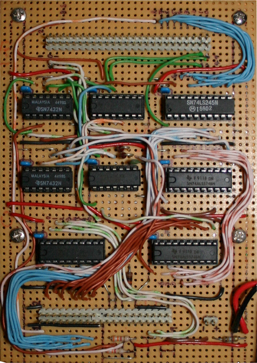
I'd always assumed the first storage device to hook up to the Z80 system would be a floppy drive. Assuming this wouldn't be too hard, I started looking for information and schematics on the Internet. Unfortunately, most of the designs I came across were based on rather ancient controller chips which you simply can't get anymore, unless you happen to find some old device from which you can salvage the required bits. It was only then that I thought about hooking up a hard disk, something I'd assumed would be much more involved and had therefore expected to add at a much later date. However, after researching the subject a little, I was pleasantly surprised to find that an ATA (a.k.a. IDE) interface was actually relatively simple to implement.
The only real proverbial spanner in the works is that the ATA interface used a 16-bit data bus, as opposed to the Z80's 8-bits. To get these to talk to each other, it's a question of using a latch to "remember" half of the 16-bit word until the other half is available. For example, to write to the ATA bus you first need to send half of your data to an 8-bit latch. The latch "remembers" this data for the time required to deliver the other half of the 16-bit word. Only when both the entire 16-bit value is available is the ATA bus called into action and signaled to read in the word in question. Reading from the bus is done using the reverse of this process, i.e. a latch stores half of the word coming from the bus until the processor's done reading the other half.
Other than this, we only need to talk to a 3-bit address bus and a couple
of control lines which in essence form one 5-bit address bus.
These lines can also be simply interfaced using a latch as we did for the
data bus. Writing to the I/O port connected to this latch can then be used
to control which of the 16 ATA registers we want to read to or write from.
The whole lot is then connected to the Z80 using a
bi-directional buffer, which makes sure the interface is islotated from
other devices on the Z80's data bus. Decoding of the Z80's address and
control busses is done using a combination of a 2-to-4 line decoder and
few logic gates. The final design (see page 4 of the
schematics ![]() ) borrows heavily from
this one
at retroleum.co.uk
) borrows heavily from
this one
at retroleum.co.uk ![]() , and
Ruud Baltissen's IDE interface for the Commodore 64
, and
Ruud Baltissen's IDE interface for the Commodore 64 ![]() .
On both of these pages you'll also find lots of useful information on using
ATA equipment on 8-bit systems.
.
On both of these pages you'll also find lots of useful information on using
ATA equipment on 8-bit systems.
Programming
Like the UART used to build the serial interface, the ATA bus makes use of registers to send data between the system and the attached devices. The first of these registers, register zero is the data register. This is where we send words to in order to write them to a device and also where we read from when fetching data. Register 1 is used when something goes wrong; should an error occur, reading register 1 should tell us the reason why. Resgister 2 is used to indicate how many sectors we want to shift around in one go, which in my case is always just the one.
Thankfully, it's no longer necessary to delve into the geometry of your ATA devices in terms of cylinders, sectors and heads. These days we can use LBA (Logical Block Addressing) to refer to the entire device as a sequential collection of sectors. On a typical hard disk, each of these sectors is 512 bytes in size and is referenced by a unique 28-bit or 48-bit address. Seeing as 28 bits gives us 228 sectors at 512 bytes each, resulting in a total of about 137GB, I was quite happy to stick with the 28-bit addressing scheme for simplicity's sake. The registers 3, 4 and 5, plus half of register 6 are used to hold the LBA address of the sector we want to work with. The other half of register 6 is used to enable or disable LBA and select either the master or the slave device.
Finally, register 7 is used to send commands to the ATA device in question. Examples of commands would be those used to initiate a read or a write, or to identify the device. The commands take the contents of the other registers as parameters, such as the LBA address, number of sectors, etc. as necessary. The rest of the registers (8 thru 15) are't of much interest in this project and can be ignored.
Using a latch for the address and control signals means a lot of this kind of thing is required to access the interface:
ld a,some_ata_register_code
out (control_port),a
in a,(ide_data_lsb_port)
Instead of repeating the information on the two pages linked to above, and pasting in hundreds of assembly code fragments, you can find my ATA driver source code in the version control repository The comments throughout should explain what's going on and why.
Troubleshooting
Building and testing the ATA interface was quite tricky. The first test of the interface was to see if I could retrieve the connected hard disk's identification info. This is a good place to start as you don't need to worry about sectors or actually accessing the storage itself. All you need to do is wait until the drive's ready, issue the right command, wait again for the drive to do its stuff, then read a 256 words (so 512 bytes) from the data ports. This was so simple, even I couldn't mess up the test program.
I did however manage to mess up a couple of things on the hardware side, which were
only really noticable when I started with my second test program. This involved
writing a known buffer to the disk, reading it back, then comparing the results.
Of course, the data read should match that just written, but to start with this
wasn't quite the case. A lot of this had to do with the delaying of signals as
they pass between the latches
and the ATA interface. This is achieved by chaining two NOT gates together with
a resistor. I'd seen confilicting examples of where these delays
should be placed, so I had a little experimentation on my hands before things
were working properly. To start with I had delays on both the /DIOR and /DIOW
lines. I also switched several times from delaying the signals so they reached
the latch before the ATA bus, and vice versa. In the end the configuration in
the schematics ![]() , with a single
delay between the latch and /DIOR, gave a reliable
result, but only after tuning the resistor's value. Strangely enough, the
prototype circuit on the bread board worked fine with a 100Ω resistor but
the stripboard version worked better with 50Ω.
, with a single
delay between the latch and /DIOR, gave a reliable
result, but only after tuning the resistor's value. Strangely enough, the
prototype circuit on the bread board worked fine with a 100Ω resistor but
the stripboard version worked better with 50Ω.
The other issue I had was whether or not fit a 3.3KΩ resistor between D7 of the ATA bus and ground. The ATA specs say you should do this, but my circuit only worked properly when this was removed.
![]()
![]()
![]()
![]()